4 Layer Pcb Design Tutorial Altium
To check the design rules. Enable the Stack Symmetry option in the Properties panel.

4 Layer Pcb Design Altium Pcb Circuits
When you need to create your PCB layer stackup the layer stack manager in Altium Designer lets you specify layer types define dielectric and core layers and configure their order in the PCB stackup.

4 layer pcb design tutorial altium. GETTING STARTED WITH PCB DESIGN. 4 Layer PCB Stackup Has Never Been Simpler with Altium Designer Dont settle for a layer stackup management tool that cant handle simple necessary requests. This tutorial is based on an astable multivibrator design.
PCB design is complex and not all design software packages have the tools to help you be successful. 0 Response to How To Make 4 Layer Pcb In Altium Post a Comment. Utilize the right PCB design software that gets your job done right the first time.
Whether youre creating a simple two-layer board or a complex high speed digital system Altium Designer has the design tools and PCB layout tutorials you need to get started and succeed. Altium Designer Tutorial 4 - PCB Layout LCD 16x2 HD44780 Tutorial 6 - 4-bit Data Transfer LCD 16x2 HD44780 Tutorial 5 - Create Custom Character November 3 October. This tutorial allows beginners to get started.
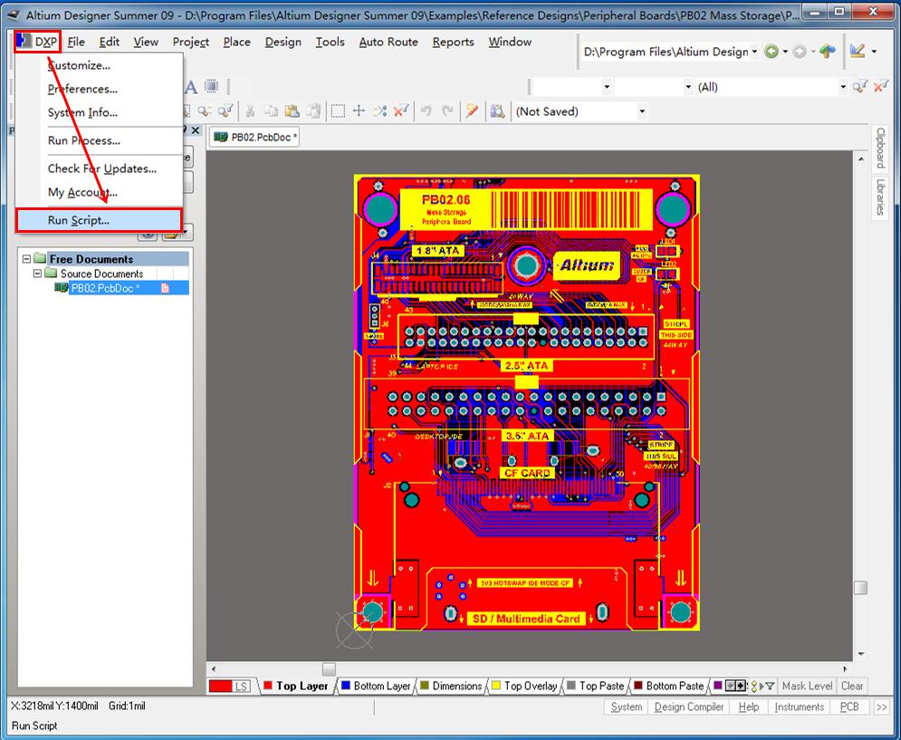
To examine and configure the layer stack for your board. 4 Layer Pcb Design In Altium For Brushless Motor Control Freelancer Edn Design Pcbs For Emi Part 2 Basic Stack Up Kenneth Wyatt We Ve Got Your Stm32mp1 Schematic Symbol Octavo Systems. The software I use is Altium Designer 13 but the basic operations are similar to other software.
I Will Design 4 Layer Pcb With Altium Designer Broxer Share this post. New users of Altium software may find value in reading the article Exploring Altium Designer for an explanation of the interface information on how to use panels and guidelines for managing design documents. Request 4 Layer PCB Quote Altium Designer 4-layer PCB Design Tutorial.
Our drones PCB should contain at least six layers. Currently the PCB stackup contains two metal layers Top and Bottom and a default dielectric layer FR-4 between them. When this option is activated the Layer Stack Manager will automatically align the top.
RS-485 This article is from a series of articles looking at some of. Altium Designer - PCB Design Software Altium 365 - PCB Design Platform Altium Nexus - Agile PCB Design FREE Trials most recent articles Serial Communications Protocols - Part Four. The PCB is double layer just for example.
Create a new project file create a related schematic file and prepare the relevant PCB design. For a new board its single default stack comprises. Embedded System Engineering Altium Designer Tutorial 4 Pcb Layout Altium Designer Pcb Design Tutorial Pcbcart Board Layers And Colors Online Documentation For Altium Products.
Four signal layers and two plane layers with a total thickness of 16 mm. Only a member of this blog may post a. Altium Designers layer stack manager makes it easy to set up an impedance profile.
Altium Designer Pcb Design Tutorial Pcbcart I Will Design 4 Layer Pcb With Altium Designer Broxer. Layer Stackup in PCB Design with Altium Designer. Open the Layer Stack Manager to do this select Design Layer Stack Manager D K.
The tutorial PCB is a simple design and can be routed as a single-sided or double-sided board. For saving spacetry to use SMT type components. The layer stack-up should be SIGNALTOPGNDPWR and SIGNALBOTTOM for 4-layer boardthat is the standard oneIf you change the order I think it will affect your proper working of circuit.
4 Layers Pcb Designing In Altium Components Placement Tutorial Planning Your Multilayer Pcb Stackup In Altium Designer. A dielectric core 2 copper layers as well as the top. Manufacturing Output Job fileStep-1 Create Assembly DrawingStep-2 3D PDFStep-3 Gerber and NC Drill FilesIf you find this video Helpful Please.
Altium Designer Pcb Design Tutorial Pcbcart The Board Altium Designer 18 1 User Manual Documentation.

4 Layers Pcb Designing In Altium Components Placement Tutorial Youtube
4 Layer Pcb Design In Altium Pcb Circuits
Altium Designer Tutorial Working With Vias And Multiple Layers Youtube
4 Layer Pcb Design Altium Pcb Circuits
